Home
Shop
Wishlist0
Sold: 0 / 50

74HC595 8-bit serial-in, serial or parallel-out shift register with output latches; 3-state

  • Low quiescent current: 80 µA maximum (74HC Series)
  • Low input current: 1 µA maximum
  • 8-bit serial-in, parallel-out shift register with storage
  • Wide operating voltage range: 2V–6V
  • Cascadable
  • Shift register has direct clear
  • Guaranteed shift frequency: DC to 30 MHz
  • Contains an 8-bit Serial-In Parallel-Out Shift Register that feeds an 8-bit D-type Storage Register
  • Shift Register has Direct Clear
  • Accurate from Dc to 20MHz
  • 3-State Outputs
  • Standard TTL Switching Voltages

Original price was: ₹54.00.Current price is: ₹42.00.

Buy Now Compare
Availability: 50 in stock

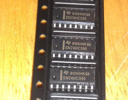
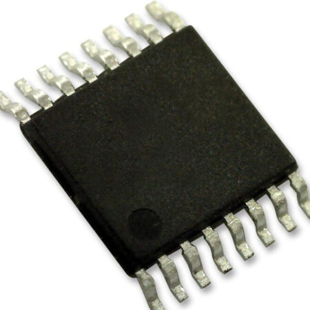
74HC595 8-bit Serial-to-Parallel Shift Register [SMD] (package: SOIC16)

Features & Specification
  • Low quiescent current: 80 µA maximum (74HC Series)
  • Low input current: 1 µA maximum
  • 8-bit serial-in, parallel-out shift register with storage
  • Wide operating voltage range: 2V–6V
  • Cascadable
  • Shift register has direct clear
  • Guaranteed shift frequency: DC to 30 MHz
  • Contains an 8-bit Serial-In Parallel-Out Shift Register that feeds an 8-bit D-type Storage Register
  • Shift Register has Direct Clear
  • Accurate from Dc to 20MHz
  • 3-State Outputs
  • Standard TTL Switching Voltages
General Description
The MM74HC595 high speed shift register utilizes advanced silicon-gate CMOS technology. This device possesses the high noise immunity and low power consumption of standard CMOS integrated circuits, as well as the ability to drive 15 LS-TTL loads.
This device contains an 8-bit serial-in, parallel-out shift register that feeds an 8-bit D-type storage register. The storage register has 8 3-STATE outputs. Separate clocks are provided for both the shift register and the storage register.
The shift register has a direct-overriding clear, serial input, and serial output (standard) pins for cascading. Both the shift register and storage register use positive-edge triggered clocks. If both clocks are connected together, the shift register state will always be one clock pulse ahead of
the storage register.
The 74HC logic family is speed, function, and pin-out compatible with the standard 74LS logic family. All inputs are protected from damage due to static discharge by internal diode clamps to VCC and ground.

 Pin Configuration

Pin Number Pin Name Description
1,2,3,4,5,6,7 Output Pins (Q1 to Q7) parallel data output
8 Ground Connected to the Ground of the circuit
9 Q7 serial data output
10 (MR) Master Reset master reset (active LOW)
11 (SH_CP) Clock This is the clock pin to which the clock signal has to be provided from MCU/MPU
12 (ST_CP) Latch The Latch pin is used to update the data to the output pins. It is active high
13 (OE) Output Enable The Output Enable is used to turn off the outputs. Must be held low for normal operation
14 (DS) Serial Data This is the pin to which data is sent, based on which the 8 outputs are controlled
15 (Q0) Output The first output pin.
16 Vcc This pin powers the IC, typically +5V is used.


FEATURES

  •  8-bit serial input
  • 8-bit serial or parallel output
  • Storage register with 3-state outputs
  • Shift register with direct clear
  • 100 MHz (typical) shift out frequency

Downloads

The 74HC595 are high-speed Si-gate CMOS devices and are pin-compatible with low power Schottky TTL (LSTTL). They are specified in compliance with JEDEC. The 74HC595 is an 8-stage serial shift register with a storage register and 3-state outputs. The shift register and storage register have separate clocks. Data is shifted on the positive-going transitions of the SH_CP input. The data in each register is transferred to the storage register on a positive-going transition of the ST_CP input. If both clocks are connected together, the shift register will always be one clock pulse ahead of the storage register. The shift register has a serial input (DS) and a serial standard output (Q7’) for cascading. It is also provided with asynchronous reset (active LOW) for all 8 shift register stages. The storage register has 8 parallel 3-state bus driver outputs. Data in the storage register appears at the output whenever the output enable input (OE) is LOW.   Pin Configuration
Pin Number Pin Name Description
1,2,3,4,5,6,7 Output Pins (Q1 to Q7) parallel data output
8 Ground Connected to the Ground of the circuit
9 Q7 serial data output
10 (MR) Master Reset master reset (active LOW)
11 (SH_CP) Clock This is the clock pin to which the clock signal has to be provided from MCU/MPU
12 (ST_CP) Latch The Latch pin is used to update the data to the output pins. It is active high
13 (OE) Output Enable The Output Enable is used to turn off the outputs. Must be held low for normal operation
14 (DS) Serial Data This is the pin to which data is sent, based on which the 8 outputs are controlled
15 (Q0) Output The first output pin.
16 Vcc This pin powers the IC, typically +5V is used.
  FEATURES
  •  8-bit serial input
  • 8-bit serial or parallel output
  • Storage register with 3-state outputs
  • Shift register with direct clear
  • 100 MHz (typical) shift out frequency
  • ESD protection:  -HBM EIA/JESD22-A114-A exceeds 2 000 V                                                           -MM EIA/JESD22-A115-A exceeds 200 V.
APPLICATIONS
  • Serial-to-parallel data conversion
  • Remote control holding register.

Reviews

There are no reviews yet.

Be the first to review “74HC595 8-bit serial-in, serial or parallel-out shift register with output latches; 3-state”

Your email address will not be published. Required fields are marked *

Back to Top
Product has been added to your cart